100 kV to 400 kV decks for positive ion beams
50 to 100s of μA of many elements from hydrogen to bismuth
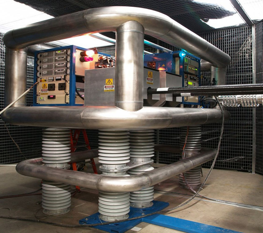
NEC High Voltage Decks produce beam current and energy that make them well suited to semiconductor implantation research and material science studies reproducing the effects of radiation damage on materials.
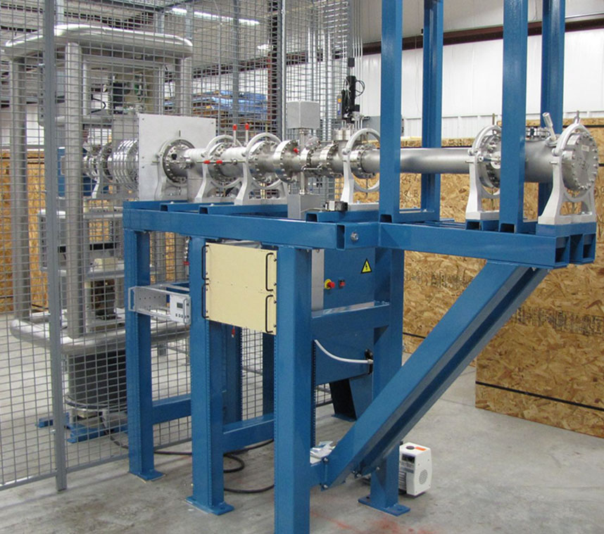
Implantation research involves depositing atoms into semiconductor wafers to modify the properties of the semiconductor. High mass resolution and beam energy control gives users a great deal of control over implant depth for depositing interstitial atoms or crystal disruption. The implantation beamlines produce high uniformity of particle flux across a wafer surface by customizable electrostatic raster scanning of the beam and exclusion of fast neutrals from the target. Implantation end stations can accommodate a variety of sample sizes, measure integrated beam current with high accuracy and wafer temperature control.
An NEC High Voltage Deck can replicate the deterioration of materials produced by energetic particles for material damage studies. Customers use HV Decks to study the suitability of materials used in high radiation areas, like fission reactors or plasma facing components in fusion reactors. The multi-beam systems can also replicate the particle fluxes hardware experiences in low earth orbit and beyond, providing valuable data on the expected long-term performance of electronics and solar panels on satellites and spacecraft. In both fields, in situ materials trials are expensive or impossible. Users can study the evolution of material damage by the precise control of particle flux, and in some applications provide accelerated testing to condense lifetime performance studies.
Because materials in these environments may experience a spectrum of particle energies and species, HV Decks can be part of a multi-beam system where a suite of systems deliver simultaneous fluxes impinging on a target. This reproduces the damage and annealing processes materials undergo in these environments. These multi-beam systems can introduce beam currents from multiple angles, or they can be part of a system with a beam mixing element (NEC patent) that delivers high energy and low energy co-axial beams on target. Several customers have used beams from High Voltage Decks to produce damage on a sample in an electron microscope to observe the evolution of materials damage in real time.
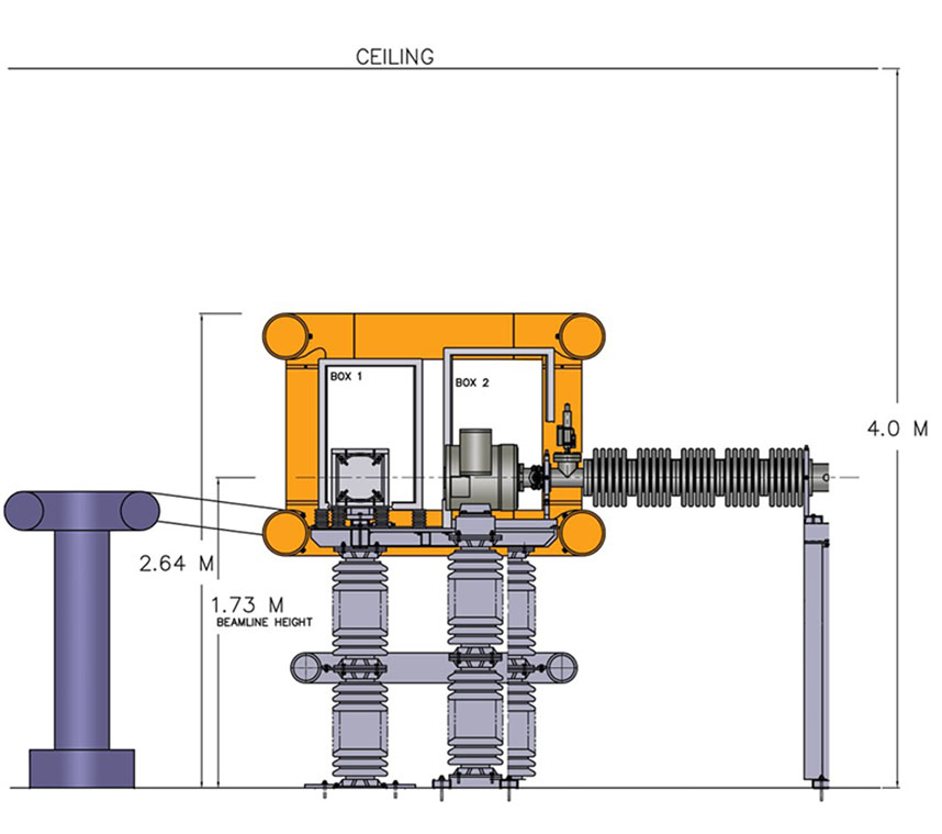
NEC manufactures high voltage decks between 100 kV and 400 kV for use in research and industry. We have also built decks up to 500 kV for use as injectors to NEC’s large vertical accelerator systems.
High voltage decks work on the same basic principles as single ended accelerator systems with one notable difference: while traditional single ended accelerators are used mainly for light ions, an HV deck can create and accelerate heavy ions with high charge states, leading to very high beam energies. Using ECR (Electron Cyclotron Resonance) or gas/sputter ion sources, NEC high voltage decks have been shown to create 100s of μA of many elements, from hydrogen to bismuth.
NEC high voltage decks also use air cooled isolation transformers or motor-generator combinations to generate power on the deck. However, this depends on specific requirements. The air-cooled isolation transformers reduce ambient noise as well as vibration for delicate experiments.
Contact NEC for more information related to these products.